- News |
-
- Featured
-
Canada’s privacy commissioner launches investigation over the use..
As the years pass by, technology also widens, and more and more are being discovered. From simple gadgets..
- Business |
-
- Featured
-
Be an informer to I-T dept; earn up..
Sharing "specific information" with the income tax department about any benami..

- Tech & Industry |
-
- Featured
-
Gravitational wave event likely signaled birth of black..
The merger of two neutron stars that generated gravitational waves detected last year may have led to the birth..

- Entertainment |
-
- Topics
- Malayalam Film
- Media
- Music
- Youth
-
- Featured
-
Shawn Mendes Released Highly Anticipated Self-Titled Album Today
Los Angeles, CA : Multi-Platinum singer/songwriter Shawn Mendes released his highly anticipated self-titled third album today, via Island Records. Get..

-
- New Products |
-
- Topics
- General
-
- Featured
-
ZOTAC Introduces Its GeForce GTX 960 series graphics..
Dubai- ZOTAC International, a leading innovator and manufacturer of graphic cards and mini-

-
- Education |
-
- Topics
- Campus News
-
- Featured
-
ITM University, Gurgaon Student Palash Chhabra Represents Varsity..
New Delhi: Palash Chhabra, a student of ITM University,..

-
- Health |
-
- Topics
- Medical News
-
- Featured
-
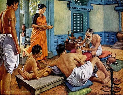
Maharshi Shushruta, The Great Grandfather of Surgery!
by Ayurvedacharya Dr.Hitesh Jani Dr.Hitesh Jani
-
- Tourism |
-
- Topics
- Travel
- Food&Beverages
- Hospitality
-
- Featured
-
“Keraliya Ayurveda is Credible and Authentic”
Irina Gurjeva Irina Gurjeva is not just another vacationer in..

-
- Sports |
- Editor's column |
- Magazine |
Manappuram conducts two day Social Security Facilitation camp
Union External Affairs Minister S Jaishankar at the International River Conference in Guwahati
Applied Materials’ New Ioniq PVD System Solves Wiring Resistance Challenges of 2D Scaling
Published on May 28, 2022
Bangalore – Applied Materials, Inc. today introduced a new system that re-engineers the deposition of transistor wiring to significantly reduce electrical resistance, which has become a critical bottleneck to further improvements in chip performance and power.

Chipmakers are using advances in lithography to shrink chips to the 3nm node and beyond. Unfortunately, as the wires become thinner, the electrical resistance increases exponentially, and this reduces chip performance and increases power consumption. If left unchecked, the wiring resistance can fully negate the benefits of more advanced transistors.
Chip wiring is deposited into trenches and vias that are etched into a dielectric material. In the conventional approach, the wiring is deposited using a metal stack that typically includes a barrier layer to prevent the metal from mixing with the dielectric; a liner layer to promote adhesion; a seed layer to facilitate metal fill; and a conductive metal like tungsten or cobalt for the transistor contacts and copper for the interconnect wires. The barriers and liners don’t scale well, so as the trenches and vias shrink, the proportion of space available for conductive metals is reduced; and the smaller the wiring, the higher the electrical resistance