- News |
-
- Featured
-
Canada’s privacy commissioner launches investigation over the use..
As the years pass by, technology also widens, and more and more are being discovered. From simple gadgets..
- Business |
-
- Featured
-
Be an informer to I-T dept; earn up..
Sharing "specific information" with the income tax department about any benami..
- Tech & Industry |
-
- Featured
-
Gravitational wave event likely signaled birth of black..
The merger of two neutron stars that generated gravitational waves detected last year may have led to the birth..

- Entertainment |
-
- Topics
- Malayalam Film
- Media
- Music
- Youth
-
- Featured
-
Shawn Mendes Released Highly Anticipated Self-Titled Album Today
Los Angeles, CA : Multi-Platinum singer/songwriter Shawn Mendes released his highly anticipated self-titled third album today, via Island Records. Get..

-
- New Products |
-
- Topics
- General
-
- Featured
-
ZOTAC Introduces Its GeForce GTX 960 series graphics..
Dubai- ZOTAC International, a leading innovator and manufacturer of graphic cards and mini-

-
- Education |
-
- Topics
- Campus News
-
- Featured
-
ITM University, Gurgaon Student Palash Chhabra Represents Varsity..
New Delhi: Palash Chhabra, a student of ITM University,..

-
- Health |
-
- Topics
- Medical News
-
- Featured
-
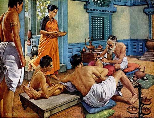
Maharshi Shushruta, The Great Grandfather of Surgery!
by Ayurvedacharya Dr.Hitesh Jani Dr.Hitesh Jani
-
- Tourism |
-
- Topics
- Travel
- Food&Beverages
- Hospitality
-
- Featured
-
“Keraliya Ayurveda is Credible and Authentic”
Irina Gurjeva Irina Gurjeva is not just another vacationer in..

-
- Sports |
- Editor's column |
- Magazine |
HHV to produce the entire Thin Film Metallized Circuit for ISRO’s Satellite program
Published on September 24, 2018
By Sachin Murdeshwar
Mumbai : Bengaluru based Hind High Vacuum Co. Pvt. Ltd. (HHV), a vacuum science and technology Company with major clients like HAL, ISRO, BARC, Titan etc,announced that is has been selected by ISRO under its technology transfer program. HHV will produce the entire Thin Film Metallized Circuit for ISRO’s Satellite program.
In 2017, HHV was awarded a ‘Certification of Qualification’ by the Space Application Center, ISRO for Thin Film Metalized substrates. Circuits are designed on these multi-layered metallized substrates and used in ISRO’s Space and Satellite program. This indigenously developed technology, as a part of HHV’s ‘Make in India’ initiative, was recognised by the Government of India and the company was  conferred with the prestigious National Research & Development Award in May, 2018.
“As a part of ISRO’s technology transfer program and as a forward integration of this award winning technology, HHV will now produce the entire Thin Film Metallized Circuit (TFMC) for ISRO’s 40-micron accuracy line, in its new technology production line known as ‘Photo Lithography’ ” said Prasanth Sakhamuri, Managing Director, HHV. “HHV has established a new Photo Lithography Lab (PLL) at its Dabaspet plant to develop TFMCs on alumina substrates that first need to be metallized in a vacuum chamber.”
Once metallized these substrates are cleaned and then coated with a photo resistive material using a spin coater. A laser writer is used to define different designs as required by customers on blank chromium mask plates. Once covered with a patterned mask plate the substrates go through ultra-violet exposure to harden exposed areas. HHV uses positive lithography to pattern and etch the metallized substrates.
A specialised etching room containing a chemical wet bench is used for multiple rounds of etching for each metallic layer. A dicing machine is then used to cut the metallized substrates to required sizes and an ISO 8 clean room is used to qualify the products. High performance microscopes and profile projectors are available for the inspection and measurement of the patterned substrates.
“The entire process requires high levels of precision and sophisticated technology to deposit coatings pattern the circuits and check the quality of the substrates within a 1000th of a millimetre. All these processes require clean room environments to ensure minimal interference with particle matter present in air. HHV’s Photo Lithography Lab has ISO 7 and ISO 8 clean rooms as well as class 100 laminar flow stations that allow us to achieve resolutions of up to 40 microns” added Prasanth Sakhamuri.
Established in 1965 at Bangalore as a specialized enterprise to develop Indian self-reliance in high vacuum technology, HHV today serves a spectrum of Industries and R&D centres covering aerospace, atomic energy, defence, automotive, semi-conductors, electrical, horology, scientific instrumentation, decorative, food processing to name a few. HHV has an advanced research and manufacturing program in thin film technology, material science, metallurgy, astronomy, and special purpose machinery.